Review the Evolution of NFC and RFID Technology and Analyze the Current Industry Status
Sort Out the Iteration Context of NFC and RFID Technology and Present the Industry Development Track
NFC and RFID Technology has experienced decades of continuous iteration and upgrading, evolving from a simple identification technology to a core support for digital transformation in various industries, and its development track has closely followed the pace of global technological progress and market demand changes. In the early stage of its birth, RFID technology, as the predecessor of NFC, mainly focused on basic identification and data collection functions, widely used in simple scenarios such as logistics labeling and asset inventory. At that time, the technology had limitations such as low data transmission rate, large equipment volume and high cost, which restricted its popularization in civilian and small and medium-sized enterprise scenarios. With the continuous breakthrough of microelectronics technology in the early 21st century, NFC technology emerged as an extension of RFID, realizing shorter-range, faster and more secure contactless communication, and gradually integrated into consumer electronic products such as mobile phones and bank cards, opening the door for its large-scale civilian application. In the past decade, driven by the rapid development of the Internet of Things, big data and artificial intelligence, NFC and RFID Technology has achieved leapfrog development: the integration of chip technology has been continuously improved, the power consumption has been significantly reduced, the application scenarios have been continuously expanded, and it has been deeply involved in retail, medical care, transportation, smart home, industrial manufacturing and many other fields. From the initial single identification function to the current multi-functional integration of data transmission, security verification, intelligent control and other functions, NFC and RFID Technology has gradually become an indispensable core link in the intelligent ecological chain, laying a solid foundation for the industry evolution towards a more intelligent, efficient and sustainable direction by 2030. Today, looking back at the evolution of NFC and RFID Technology, each iteration is a response to market demand and a breakthrough in technological bottlenecks, and this development momentum will continue to promote the continuous innovation of the industry in the future.
Summarize the Current Pain Points of Technology Application and Industry Development Bottlenecks
While NFC and RFID Technology has achieved remarkable development and wide application, it still faces many pain points in practical application and bottlenecks restricting industry development, which need to be solved in the process of moving towards 2030. In terms of technology application, the first pain point is the inconsistency of technical standards. Due to the lack of unified global technical specifications, different enterprises and industries adopt different communication protocols, frequency bands and data formats, resulting in poor compatibility between NFC/RFID products of different brands and difficulty in realizing interconnection and intercommunication, which greatly limits the expansion of application scenarios and the formation of industrial ecology. Secondly, the performance of the technology still has room for improvement. In some complex application scenarios such as high-density asset management and harsh industrial environments, the data transmission stability of NFC and RFID Technology is insufficient, and the reading distance and accuracy are easily affected by environmental factors such as electromagnetic interference and obstacles, which affects the user experience and application effect. Thirdly, the cost control is difficult. For small and medium-sized enterprises, the initial investment cost of NFC/RFID equipment, chip procurement and system deployment is relatively high, and the later operation and maintenance cost also increases the enterprise’s financial burden, making it difficult for many small and medium-sized enterprises to popularize and apply the technology on a large scale. In terms of industry development, the bottlenecks are mainly reflected in three aspects: first, the lack of core technical patents, most of the high-end chip and key component technologies are monopolized by a few international enterprises, which restricts the independent innovation capacity and industrial competitiveness of the global industry; second, the talent gap is obvious, the industry needs a large number of professional talents who master both NFC and RFID Technology and industry application scenarios, but the current talent training speed can not keep up with the pace of industry development; third, the application depth is insufficient, most industries still stay in the basic application stage of identification and data collection, and the deep integration with emerging technologies such as artificial intelligence and 5G is not enough, which can not give full play to the maximum value of NFC and RFID Technology. These pain points and bottlenecks are not only the key problems that the industry needs to solve at present, but also the important direction of technological innovation and industrial upgrading before 2030.
Interpret the Technology Standardization Process and Current Market Application Pattern
The standardization process of NFC and RFID Technology is an important guarantee for the healthy and orderly development of the industry, and it is also an important factor affecting the market application pattern. In recent years, with the joint efforts of global industry organizations, enterprises and research institutions, the standardization of NFC and RFID Technology has made remarkable progress. Internationally, organizations such as ISO/IEC, ETSI and GSMA have formulated a series of technical standards covering communication protocols, frequency bands, data formats and security specifications, which have laid a foundation for the interconnection and intercommunication of products in different regions and industries. For example, ISO/IEC 14443 standard defines the technical parameters of NFC near-field communication, which has become the global mainstream standard for civilian NFC products; ISO/IEC 18000 standard specifies the technical requirements of RFID technology in different frequency bands, providing a unified standard for the application of RFID in logistics, retail and other fields. Domestically, relevant national departments and industry associations have also formulated a number of industry standards and national standards, which are closely combined with the actual application needs of the domestic market, and have promoted the localized development and application of NFC and RFID Technology. At present, the standardization process of NFC and RFID Technology is gradually moving towards global unification and refinement, and more detailed and targeted standards will be formulated for different application scenarios in the future, further promoting the integration and development of the industry. In terms of the current market application pattern, the global NFC/RFID market presents a pattern of “dominance by leading enterprises and gradual rise of emerging enterprises”. From the perspective of market segments, the RFID market is mainly concentrated in logistics and supply chain management, retail inventory management and industrial asset management, accounting for more than 60% of the total market share; the NFC market is mainly focused on consumer electronics, mobile payment, smart access control and other civilian fields, with the rapid popularization of smart phones, the market scale is growing at a high speed every year. From the perspective of regional distribution, North America, Europe and Asia-Pacific are the three major market regions in the world. North America and Europe have a high degree of technological maturity and a large market scale, mainly dominated by high-end applications; the Asia-Pacific region has the fastest growth rate, driven by the rapid development of emerging economies such as China and India, with strong market potential, and has gradually become a global manufacturing and application center of NFC/RFID products. In terms of enterprise competition, international leading enterprises such as NXP, Intel and Texas Instruments occupy a dominant position in the high-end chip and core component market, while a large number of domestic enterprises are mainly engaged in the research and development, production and application of middle and low-end products, and are gradually strengthening independent innovation, constantly narrowing the gap with international leading enterprises. With the acceleration of the standardization process and the continuous expansion of application scenarios, the market application pattern of NFC and RFID Technology will be further optimized, and the market competition will be more intense and standardized.
Look Forward to the Core Development Directions of NFC/RFID Chip Technology in 2030
Continuous Breakthrough in Chip Data Transmission Rate to Achieve Performance Leap
Chip technology is the core of NFC and RFID Technology, and the data transmission rate is one of the key performance indicators of NFC/RFID chips, which directly affects the application effect and efficiency of the technology. Looking forward to 2030, the data transmission rate of NFC/RFID chips will achieve continuous breakthroughs, realizing a qualitative leap in performance, and providing strong support for the expansion of more high-end and complex application scenarios. At present, the data transmission rate of mainstream NFC chips is about 424 kbps, and the data transmission rate of RFID chips in the UHF band is about 100 kbps to 1 Mbps, which can basically meet the needs of basic application scenarios such as identification and simple data transmission, but it is difficult to meet the needs of high-speed data transmission in complex scenarios such as real-time video transmission, large-capacity data interaction and high-density concurrent reading. Before 2030, with the continuous progress of microelectronics technology, nanotechnology and communication technology, the data transmission rate of NFC/RFID chips will be increased to 10 Mbps or even higher, which is dozens of times higher than the current level. This breakthrough will not only greatly improve the efficiency of data transmission, shorten the interaction time between equipment, but also enable NFC and RFID Technology to realize more complex functions, such as real-time transmission of high-definition video data in intelligent monitoring scenarios, large-capacity data synchronization in medical equipment, and high-density concurrent reading in large-scale events. In addition, while improving the data transmission rate, the power consumption of NFC/RFID chips will also be further reduced through technological innovation. Through the optimization of chip structure design, the adoption of low-power materials and the improvement of power management technology, the power consumption of chips will be reduced by more than 50% compared with the current level, which will extend the service life of passive NFC/RFID tags and equipment, and expand the application scope of the technology in scenarios with limited power supply such as outdoor assets and wearable devices. The continuous breakthrough of chip data transmission rate and the leap of performance will inject new vitality into the development of NFC and RFID Technology, and promote the technology to move towards a more efficient, fast and low-power direction.
Flexible Chips Become Mainstream to Adapt to Diverse and Complex Application Scenarios
With the continuous expansion of NFC and RFID Technology application scenarios, the demand for chip form factors is becoming more and more diverse. The traditional rigid chips are limited by their shape and material characteristics, and it is difficult to adapt to complex application scenarios such as curved surfaces, irregular objects and wearable devices. Looking forward to 2030, flexible chips will become the mainstream of NFC/RFID chips, with their unique flexibility and ductility, adapting to various diverse and complex application scenarios, and further expanding the application boundary of NFC and RFID Technology. Flexible NFC/RFID chips are made of flexible electronic materials such as organic semiconductors and flexible substrates, which can be bent, folded and stretched without affecting their performance, and can be closely attached to the surface of various irregular objects, such as curved product packaging, clothing fabrics, human skin and automotive parts. In the field of wearable devices, flexible NFC/RFID chips can be integrated into smart bracelets, smart clothes, smart shoes and other products, realizing functions such as health data monitoring, identity verification and mobile payment, and bringing a more convenient and comfortable user experience; in the field of intelligent packaging, flexible chips can be embedded into curved packaging boxes and flexible packaging bags, realizing product anti-counterfeiting, traceability and inventory management, and improving the intelligence level of the packaging industry; in the field of medical care, flexible chips can be made into flexible tags attached to medical devices and human bodies, realizing real-time monitoring of medical device usage and patient health data, and improving the efficiency and safety of medical services. In addition, flexible NFC/RFID chips also have the advantages of light weight, thin thickness and low cost, which can be mass-produced through innovative manufacturing processes, further reducing the application cost and promoting the large-scale popularization of the technology in more fields. Before 2030, with the continuous maturity of flexible electronic technology, the performance of flexible NFC/RFID chips will be further improved, the application cost will be further reduced, and they will gradually replace traditional rigid chips to become the mainstream of the market, promoting the in-depth integration of NFC and RFID Technology with more diverse and complex application scenarios, and creating more new application models and industrial opportunities.
Strengthen the Chip Security Architecture to Resist New Cybersecurity Threats
With the widespread application of NFC and RFID Technology in financial payment, personal identification, medical health and other sensitive fields, the security of chips has become an increasingly important issue. In recent years, with the continuous upgrading of cyber attack technologies, NFC/RFID chips are facing more and more new cybersecurity threats, such as data leakage, tampering, counterfeiting and unauthorized access, which have brought hidden dangers to the legitimate rights and interests of users and the healthy development of the industry. Looking forward to 2030, strengthening the chip security architecture will become one of the core development directions of NFC/RFID chip technology, and a more comprehensive and reliable security protection system will be built to effectively resist new cybersecurity threats. In the future, NFC/RFID chips will adopt a multi-level security architecture design, integrating hardware security, software security and protocol security to form a full-chain security protection. In terms of hardware security, advanced encryption chips and security modules will be integrated into the chip, adopting military-grade encryption algorithms to encrypt data storage and transmission, preventing data leakage and tampering; at the same time, physical anti-attack technologies such as anti-disassembly, anti-debugging and anti-counterfeiting will be adopted to prevent the chip from being physically attacked and counterfeited. In terms of software security, a more perfect security operating system and security management mechanism will be built, strengthening the security verification of data access and operation, and preventing unauthorized access and operation; at the same time, regular security updates and patches will be provided to timely fix security vulnerabilities and resist new cyber attack technologies. In terms of protocol security, more secure communication protocols will be adopted, optimizing the security mechanism of data interaction, and preventing data from being intercepted and tampered during transmission. In addition, the future NFC/RFID chips will also integrate biometric identification technologies such as fingerprint recognition and face recognition, realizing multi-factor authentication, further improving the security of identity verification and preventing identity theft. With the continuous strengthening of the chip security architecture, the security performance of NFC and RFID Technology will be greatly improved, which will effectively resolve cybersecurity threats, enhance user trust, and promote the technology to be applied in more sensitive and high-security demand fields, such as financial services, national defense and military industry.
Explore the Innovation of Emerging Materials and Manufacturing Processes for NFC/RFID in 2030
New Flexible Materials Promote More Lightweight and Flexible Tag Forms
The form of NFC/RFID tags is closely related to the materials used, and the innovation of materials is an important driving force for the upgrading of tag forms. Looking forward to 2030, the emergence and application of new flexible materials will promote the form of NFC/RFID tags to become more lightweight, flexible and diverse, breaking the limitations of traditional tag forms and adapting to more complex and personalized application scenarios. At present, most NFC/RFID tags are made of rigid materials such as plastic and paper, which have the disadvantages of heavy weight, poor flexibility and single form, and are difficult to adapt to the application needs of curved surfaces, irregular objects and wearable devices. In the future, new flexible materials such as graphene, carbon nanotubes, flexible organic semiconductors and biodegradable polymers will be widely used in the production of NFC/RFID tags. Graphene, as a new type of two-dimensional material, has the advantages of ultra-thin, ultra-light, high flexibility, high conductivity and high strength. Applying graphene to NFC/RFID tags can greatly reduce the thickness and weight of tags, improve the flexibility and conductivity of tags, and make tags can be bent, folded and stretched at will without affecting their performance. Carbon nanotubes have excellent electrical conductivity and mechanical properties, which can improve the data transmission efficiency and durability of tags, and make tags can work stably in harsh environments. Flexible organic semiconductors have the advantages of low cost, easy processing and good flexibility, which can realize the mass production of flexible tags and reduce the application cost. Biodegradable polymers can solve the environmental pollution problem caused by traditional plastic tags, and realize the green and environmentally friendly development of tags. With the application of these new flexible materials, the form of NFC/RFID tags will be greatly innovated: ultra-thin tags with a thickness of less than 0.1 millimeters can be attached to the surface of various materials; flexible tags can be integrated into clothing, fabrics and other products; stretchable tags can be applied to wearable devices and human skin; biodegradable tags can be used in disposable products such as food packaging, reducing environmental pollution. These new forms of tags will further expand the application scope of NFC and RFID Technology, making the technology penetrate into every aspect of people’s life and production, and bringing more convenient and intelligent services.
Innovative Manufacturing Processes Improve Chip Production Capacity and Reduce Production Costs
The manufacturing process of NFC/RFID chips and tags is directly related to production capacity, product quality and production costs, and is an important factor affecting the large-scale popularization of the technology. Looking forward to 2030, innovative manufacturing processes will be widely applied in the field of NFC/RFID, greatly improving chip production capacity, reducing production costs, and promoting the healthy and rapid development of the industry. At present, the manufacturing of NFC/RFID chips mainly adopts traditional semiconductor manufacturing processes, which have the disadvantages of complex process, high production cost and limited production capacity, and it is difficult to meet the growing market demand; the production of tags mainly adopts traditional printing and packaging processes, which have low production efficiency and poor product consistency. In the future, a series of innovative manufacturing processes will be applied to the production of NFC/RFID chips and tags. In terms of chip manufacturing, the 3D stacking process will become the mainstream. This process can stack multiple chip layers vertically, integrating more functions on a smaller chip area, not only improving the performance and integration of chips, but also reducing the chip size and production cost; at the same time, the 3D stacking process can greatly improve production efficiency and production capacity, meeting the large-scale market demand. In addition, the flexible printing electronics process will also be applied to the manufacturing of flexible chips. This process can print electronic circuits and chips on flexible substrates through inkjet printing, screen printing and other methods, which has the advantages of low cost, high efficiency and mass production, and can realize the large-scale production of flexible chips. In terms of tag manufacturing, the roll-to-roll (R2R) printing process will be widely used. This process can realize continuous printing, coating and cutting of tags on flexible substrates, greatly improving production efficiency, reducing production costs, and ensuring product consistency; at the same time, the R2R printing process can be combined with new flexible materials to produce various forms of flexible tags, adapting to different application scenarios. In addition, the application of intelligent manufacturing technologies such as industrial robots and artificial intelligence in the production process will further improve production efficiency, reduce manual intervention, and improve product quality and yield. With the application of these innovative manufacturing processes, the production capacity of NFC/RFID chips and tags will be greatly improved, the production cost will be significantly reduced, making the technology more affordable for small and medium-sized enterprises and individual users, and promoting the large-scale popularization and application of NFC and RFID Technology in more fields.
Application of Environmental Protection Materials Realizes Low-Carbon Transformation in the Manufacturing Link
Against the background of global carbon neutrality and green development, the low-carbon transformation of various industries has become an inevitable trend, and the NFC/RFID industry is no exception. Looking forward to 2030, the wide application of environmental protection materials in the manufacturing link of NFC/RFID chips and tags will realize the low-carbon transformation of the industry, promote the green and sustainable development of the industry, and respond to the global call for environmental protection. At present, the manufacturing of NFC/RFID chips and tags mainly uses non-environmentally friendly materials such as plastic, metal and chemical solvents, which will produce a lot of waste gas, waste water and solid waste during the production process, causing environmental pollution; at the same time, a large number of discarded tags will also become white pollution, causing serious damage to the ecological environment. In the future, the NFC/RFID industry will vigorously promote the application of environmental protection materials, replacing traditional non-environmentally friendly materials with green, low-carbon and biodegradable materials. In terms of chip manufacturing, environmentally friendly semiconductor materials such as gallium nitride and silicon carbide will be adopted, which not only have excellent performance, but also have lower energy consumption and less environmental pollution during the manufacturing process; at the same time, the use of toxic and harmful chemical solvents will be reduced, and environmentally friendly process solvents will be adopted to reduce environmental pollution. In terms of tag manufacturing, biodegradable materials such as corn starch, polylactic acid (PLA) and chitosan will be widely used to replace traditional plastic materials. These biodegradable materials can be naturally degraded in the natural environment after being discarded, without causing white pollution, and realizing the green cycle of tags. In addition, recyclable materials will also be applied to the production of tags. The metal materials and electronic components in the tags can be recycled and reused after being discarded, reducing the waste of resources and the cost of raw materials. In addition to the application of environmental protection materials, the manufacturing process of NFC/RFID will also be optimized to realize low-carbon production. By improving the production process, reducing energy consumption and waste emission, and adopting clean energy such as solar energy and wind energy to power the production line, the carbon emission of the manufacturing link will be greatly reduced. Looking forward to 2030, with the application of environmental protection materials and the optimization of low-carbon processes, the NFC/RFID industry will achieve a comprehensive low-carbon transformation, realizing the coordinated development of industrial development and environmental protection, and making positive contributions to global carbon neutrality.
Focus on the Energy Efficiency and Sustainable Development Path of NFC/RFID in 2030
Optimize Passive Power Supply Technology to Improve Equipment Energy Utilization Efficiency
Energy efficiency is an important indicator of the sustainable development of NFC and RFID Technology, especially for passive NFC/RFID tags and equipment that do not have an independent power supply. Looking forward to 2030, optimizing passive power supply technology will become an important direction to improve the energy utilization efficiency of NFC/RFID equipment, extend the service life of equipment, and promote the sustainable development of the technology. At present, passive NFC/RFID tags mainly rely on the electromagnetic field emitted by the reader to obtain energy, but the current passive power supply technology has the disadvantages of low energy conversion efficiency and poor energy collection capacity, resulting in the tags can only work in a short distance, and the service life is limited in complex environments. In the future, the passive power supply technology of NFC/RFID will be comprehensively optimized through technological innovation. On the one hand, the energy collection module of the tag will be improved, adopting more efficient energy conversion materials and structures, improving the efficiency of converting electromagnetic energy into electrical energy, so that the tag can collect more energy in the same electromagnetic field environment, extending the reading distance and working time of the tag. For example, the application of new energy collection materials such as graphene can greatly improve the energy conversion efficiency of the tag, making the tag can work stably at a longer distance. On the other hand, the power management technology of the tag will be optimized, adopting an intelligent power management chip to reasonably allocate and use the collected energy, reducing energy waste. The intelligent power management chip can automatically adjust the working state of the tag according to the energy supply, enter the low-power standby state when there is no data interaction, and quickly wake up when data interaction is needed, maximizing the use of limited energy. In addition, the multi-source energy collection technology will be introduced into passive NFC/RFID tags, which can collect energy from multiple sources such as solar energy, ambient light and radio frequency signals at the same time, improving the stability and reliability of the tag’s energy supply. For example, in outdoor scenarios, the tag can collect solar energy and radio frequency energy at the same time, ensuring continuous and stable work; in indoor scenarios, the tag can collect ambient light energy and electromagnetic field energy, meeting the working needs of different environments. With the optimization of passive power supply technology, the energy utilization efficiency of NFC/RFID equipment will be greatly improved, the service life of passive tags will be significantly extended, and the application scope of the technology will be further expanded, especially in outdoor, remote and other scenarios with limited power supply, promoting the sustainable development of technology.
Build a Full-Life-Cycle Recyclable Technology Product System
Building a full-life-cycle recyclable product system is an important part of the sustainable development of NFC and RFID Technology, which can not only reduce resource waste and environmental pollution, but also reduce production costs and improve the economic benefits of the industry. Looking forward to 2030, the NFC/RFID industry will focus on building a full-life-cycle recyclable technology product system, covering the entire process from product design, production, use to recycling and reuse, realizing the green cycle of products. In terms of product design, the concept of recyclability will be integrated into the design of NFC/RFID chips, tags and equipment. The product structure will be designed to be easy to disassemble and assemble, so that the various components of the product can be easily separated and recycled; at the same time, the selection of materials will prioritize recyclable and biodegradable materials, ensuring that the product can be recycled or naturally degraded after being discarded. For example, the design of NFC/RFID tags will adopt a detachable structure, and the chip and metal antenna can be easily separated from the substrate, facilitating the recycling and reuse of the chip and antenna; the substrate will adopt biodegradable materials, which can be naturally degraded after being discarded, reducing environmental pollution. In terms of production, the production process will be optimized to reduce the generation of waste and improve the utilization rate of raw materials; at the same time, the waste generated in the production process will be recycled and reused, realizing the resource utilization of waste. For example, the waste materials generated in the chip manufacturing process will be recycled and processed, and reused in the production of low-end chips or other products; the waste water and waste gas generated in the production process will be treated to meet the environmental protection standards before being discharged. In terms of use, the service life of NFC/RFID products will be extended through technological innovation and quality improvement, reducing the frequency of product replacement; at the same time, the functions of products will be upgraded through software updates, avoiding the waste caused by the obsolescence of hardware functions. In terms of recycling and reuse, a complete product recycling system will be established, including recycling channels, recycling mechanisms and recycling technologies. Enterprises will set up special recycling points to recycle discarded NFC/RFID products; professional recycling enterprises will process the recycled products, separate and extract usable components such as chips and antennas, and reuse them in the production of new products; for products that cannot be recycled, they will be treated in an environmentally friendly way to reduce environmental pollution. Looking forward to 2030, with the improvement of the full-life-cycle recyclable product system, the NFC/RFID industry will realize the green and sustainable development of products, reducing resource waste and environmental pollution, and promoting the coordinated development of the industry and the environment.
Promote the Implementation of Circular Economy Development
in the Industry with Low-Carbon Design
Low-carbon design is an important means to promote the circular economy development of the NFC/RFID industry, and it is also an important way to achieve the global carbon neutrality goal. Looking forward to 2030, the NFC/RFID industry will take low-carbon design as the core, promote the integration of low-carbon concepts into the entire industrial chain, and promote the implementation of circular economy development in the industry. Circular economy, as a development model of “resource – product – renewable resource”, focuses on reducing resource consumption, reducing waste generation and realizing resource recycling, which is highly consistent with the low-carbon development needs of the NFC/RFID industry. In the future, low-carbon design will run through the entire industrial chain of NFC/RFID, including product design, material selection, production manufacturing, product use and recycling. In product design, the principle of “energy conservation, emission reduction and recycling” will be adhered to, optimizing the product structure and function, reducing the energy consumption and resource consumption of the product during use and production. For example, the design of NFC/RFID chips will adopt low-power design, reducing the energy consumption of the chip during work; the design of tags will adopt lightweight and miniaturized design, reducing the use of raw materials. In material selection, priority will be given to low-carbon, environmentally friendly and recyclable materials, reducing the use of high-carbon and non-environmentally friendly materials, and reducing the carbon emission generated during the material production process. For example, replacing traditional high-carbon metal materials with low-carbon alloy materials, and replacing plastic materials with biodegradable materials, reducing the carbon footprint of products. In production manufacturing, clean production technologies and low-carbon production processes will be adopted, reducing energy consumption and carbon emissions during production. For example, using clean energy such as solar energy and wind energy to power the production line, optimizing the production process to reduce waste gas, waste water and solid waste emissions, and improving the utilization rate of raw materials. In product use, the service life of products will be extended, and the energy utilization efficiency of products will be improved, reducing the frequency of product replacement and the generation of waste. For example, through the optimization of passive power supply technology, the service life of passive tags is extended, reducing the number of discarded tags; through the intelligent management of equipment, the energy consumption of equipment during use is reduced. In recycling, a complete recycling system will be established, promoting the recycling and reuse of discarded products, realizing the resource utilization of waste, and reducing the carbon emission generated by the disposal of waste products. Looking forward to 2030, with the in-depth promotion of low-carbon design, the NFC/RFID industry will gradually form a circular economy development model, realizing the coordinated development of economic benefits, social benefits and environmental benefits, and making positive contributions to the global circular economy and carbon neutrality cause.
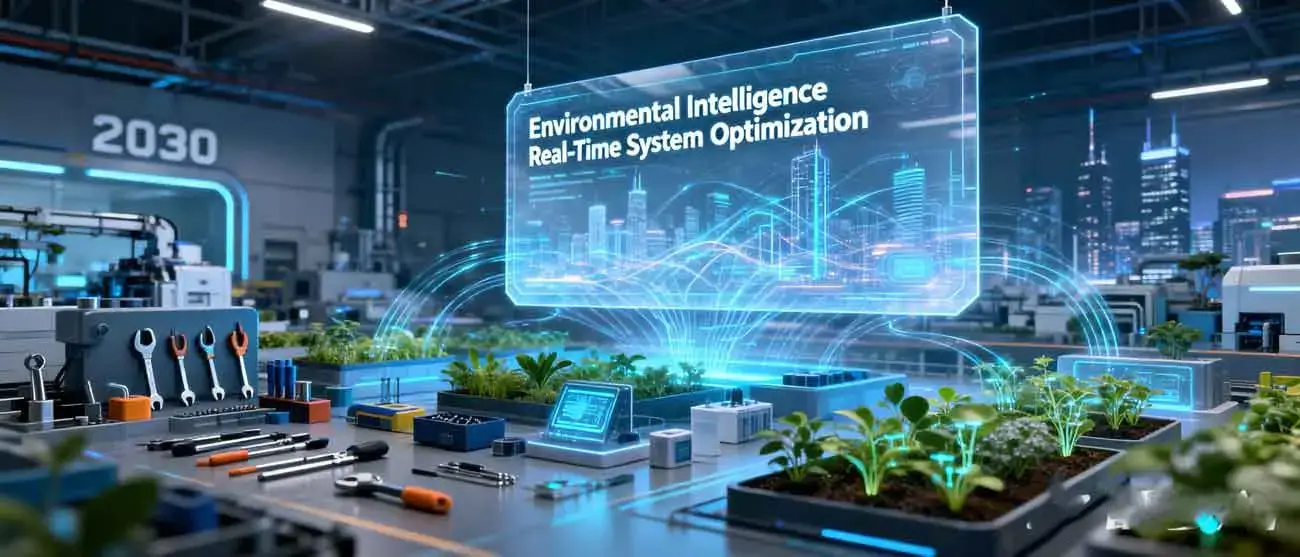
Look Forward to the In-Depth Integration Application of 5G/6G Network and Internet of Things in 2030
Rely on 5G/6G High-Speed Transmission to Realize the Upgrade of the Internet of Everything Scenario
The integration of NFC and RFID Technology with 5G/6G network and Internet of Things is an important trend in the development of the industry, and it is also an important way to expand the application boundary of the technology. Looking forward to 2030, with the large-scale popularization and application of 5G/6G network, NFC and RFID Technology will rely on the high-speed transmission, low latency and large connection characteristics of 5G/6G, realize the upgrade of the Internet of Everything scenario, and promote the formation of a more intelligent and efficient industrial ecology. At present, the integration of NFC and RFID Technology with 4G network and Internet of Things has achieved some results, but due to the limitations of 4G network in transmission speed, latency and connection number, it is difficult to meet the needs of high-speed, real-time and large-scale Internet of Everything scenarios. In 2030, 5G will become the global mainstream communication network, and 6G will start trial operation and commercialization. 5G/6G network has the characteristics of ultra-high speed (transmission rate up to 100 Gbps), ultra-low latency (latency less than 1 ms) and ultra-large connection (1 million connections per square kilometer), which can perfectly make up for the shortcomings of current network technology and provide strong support for the in-depth integration of NFC and RFID Technology and Internet of Things. Relying on 5G/6G high-speed transmission, NFC and RFID Technology can realize real-time transmission of large-capacity data, such as high-definition video, large-scale sensor data and complex control signals, which can promote the upgrade of various Internet of Everything scenarios. In the field of intelligent transportation, NFC/RFID tags installed on vehicles, roads and traffic facilities can collect real-time traffic data, and transmit the data to the intelligent traffic management platform in real time through 5G/6G network, realizing real-time traffic scheduling, intelligent parking and autonomous driving, improving traffic efficiency and safety; in the field of smart city, NFC and RFID Technology can be integrated with various urban infrastructure, collecting real-time data of water supply, power supply, gas supply and environmental protection, and transmitting the data to the smart city management platform through 5G/6G network, realizing intelligent management of the city and improving the quality of urban life; in the field of industrial Internet, NFC/RFID tags installed on industrial equipment and products can collect real-time production data and asset status data, and transmit the data to the industrial control platform in real time through 5G/6G network, realizing intelligent production, predictive maintenance and full-life-cycle management of products, improving production efficiency and reducing production costs. With the support of 5G/6G network, the Internet of Everything scenario based on NFC and RFID Technology will be comprehensively upgraded, moving towards a more intelligent, efficient and real-time direction.
Promote the Seamless Connection between Technology and Internet of Things Ecology to Expand the Application Boundary
Looking forward to 2030, promoting the seamless connection between NFC and RFID Technology and Internet of Things ecology will become an important direction to expand the application boundary of the technology, realize the interconnection and intercommunication of all things, and build a more comprehensive intelligent ecological system. At present, although NFC and RFID Technology has been widely applied in various fields of the Internet of Things, there is still a problem of “information island” between different application systems and different products, and the seamless connection between technology and Internet of Things ecology has not been realized, which limits the expansion of application boundaries and the play of technological value. In 2030, with the continuous improvement of the Internet of Things ecology and the acceleration of the standardization process of NFC and RFID Technology, the seamless connection between the two will be gradually realized. On the one hand, the technical standards of NFC/RFID will be further unified, and the compatibility between different products and systems will be improved, realizing the interconnection and intercommunication of data between different application scenarios. For example, the NFC/RFID tags used in logistics, retail and medical care will adopt the same data format and communication protocol, realizing the sharing and interconnection of data between different industries, and promoting the formation of a cross-industry Internet of Things ecological chain. On the other hand, NFC and RFID Technology will be deeply integrated with various Internet of Things platforms, such as cloud computing platforms, big data analysis platforms and intelligent control platforms, realizing the seamless connection of technology and ecology. For example, the data collected by NFC/RFID tags will be uploaded to the cloud computing platform in real time, processed and analyzed by the big data analysis platform, and the analysis results will be transmitted to the intelligent control platform to realize intelligent decision-making and control. In addition, NFC and RFID Technology will be integrated with other Internet of Things technologies such as sensors, Bluetooth and ZigBee, forming a multi-technology fusion application model, expanding the application boundary of the technology. For example, in the field of smart home, NFC and RFID Technology can be integrated with Bluetooth and sensor technology, realizing intelligent control of home appliances, intelligent security and intelligent environment monitoring; in the field of medical health, NFC and RFID Technology can be integrated with sensor and 5G technology, realizing real-time monitoring of patient health data, remote diagnosis and intelligent medical care. With the seamless connection between NFC and RFID Technology and Internet of Things ecology, the application boundary of the technology will be further expanded, penetrating into more fields and scenarios, and building a more comprehensive, intelligent and interconnected Internet of Things ecological system.
Realize Multiple Functions Triggered by a Single Interaction in Multiple Scenarios to Improve Convenience
Improving user convenience is one of the core goals of the development of NFC and RFID Technology. Looking forward to 2030, with the in-depth integration of NFC and RFID Technology with 5G/6G network and Internet of Things, it will realize multiple functions triggered by a single interaction in multiple scenarios, greatly improving user convenience and enhancing user experience. At present, the application of NFC and RFID Technology in most scenarios still stays in the single-function stage, that is, a single interaction can only realize one function, such as identification, payment or data collection, which can not meet the user’s demand for multi-functional and convenient services. In 2030, with the improvement of technology performance and the optimization of the Internet of Things ecological system, NFC and RFID Technology will realize the function of “one touch, multiple services”, that is, a single interaction between the user and the NFC/RFID tag or equipment can trigger multiple related functions, realizing multi-functional integration and improving service efficiency and convenience. For example, in the smart travel scenario, when the user touches the NFC/RFID tag at the bus station with a smart phone, a single interaction can trigger multiple functions at the same time: querying the real-time arrival time of the bus, purchasing bus tickets, planning the travel route, and synchronizing the travel information to the user’s calendar, realizing one-stop travel service; in the smart shopping scenario, when the user touches the NFC/RFID tag on the product with a smart phone, a single interaction can trigger functions such as querying product details, checking product authenticity, comparing prices, adding to the shopping cart and making payments, realizing one-stop shopping service; in the smart office scenario, when the user touches the NFC/RFID tag at the office door with a work card, a single interaction can trigger functions such as opening the door, turning on the office equipment, logging in to the office system and checking the work schedule, realizing one-stop office service; in the smart home scenario, when the user touches the NFC/RFID tag on the wall with a smart remote control, a single interaction can trigger functions such as turning on the lights, adjusting the air conditioning temperature, opening the curtains and playing music, realizing intelligent control of the home environment. The realization of multiple functions triggered by a single interaction is inseparable from the support of 5G/6G high-speed transmission and the Internet of Things ecological system. 5G/6G network ensures the real-time transmission of multi-functional data, and the Internet of Things ecological system realizes the linkage between different devices and functions, making the multi-functional integration of a single interaction possible. This function will not only greatly improve user convenience, reduce the user’s operation steps, but also promote the popularization and application of NFC and RFID Technology in more civilian scenarios, making the technology closely integrated with people’s daily life and bringing a more intelligent and convenient life experience to users.
Layout the Integrated Development Direction of Artificial Intelligence and Edge Computing in 2030
The Combination of AI and RFID Improves the Accuracy of Object Positioning and Tracking
Object positioning and tracking is one of the important application scenarios of NFC and RFID Technology, and the combination with artificial intelligence (AI) will greatly improve the accuracy and efficiency of positioning and tracking. Looking forward to 2030, the in-depth combination of AI and RFID will become an important development direction, realizing high-precision positioning and real-time tracking of objects in complex scenarios, and expanding the application value of the technology. At present, the RFID positioning and tracking technology mainly adopts methods such as signal strength (RSSI), time difference of arrival (TDOA) and angle of arrival (AOA), but these methods have the disadvantages of low positioning accuracy and poor anti-interference ability, and it is difficult to meet the positioning needs of complex scenarios such as high-density environments and dynamic objects. In 2030, with the rapid development of AI technology, especially the maturity of machine learning, deep learning and computer vision technology, the combination of AI and RFID will solve the current shortcomings of positioning and tracking technology. On the one hand, AI technology will be used to optimize the RFID positioning algorithm. Through machine learning algorithms, a large amount of historical positioning data and environmental data will be analyzed and learned, establishing a positioning model adapted to different environments, which can automatically adjust the positioning parameters according to the changes of the environment, improving the positioning accuracy and anti-interference ability. For example, in a high-density warehouse environment, the AI algorithm can analyze the interference factors such as signal reflection and shielding, and correct the positioning data in real time, realizing the high-precision positioning of goods; in a dynamic environment such as logistics transportation, the AI algorithm can predict the movement trajectory of objects according to the historical movement data of objects, realizing real-time tracking and trajectory prediction of objects. On the other hand, the combination of AI and computer vision technology will further improve the accuracy of RFID positioning and tracking. By integrating RFID tags with cameras, the AI algorithm can fuse the data collected by RFID and the image data collected by cameras, realizing multi-dimensional positioning and tracking of objects. For example, in the field of public security, RFID tags installed on suspects or key objects can be used to collect position data, and cameras can be used to collect image data. The AI algorithm fuses the two types of data to accurately determine the position and movement trajectory of objects, helping the public security department to quickly track and capture suspects. In addition, AI technology can also realize intelligent analysis of positioning and tracking data, such as identifying abnormal movement of objects, predicting the loss risk of objects, and providing targeted early warning and suggestions. Looking forward to 2030, the combination of AI and RFID will greatly improve the accuracy and efficiency of object positioning and tracking, making the technology widely applied in logistics, public security, industrial manufacturing, medical care and other fields, bringing more intelligent and efficient services.
Edge Computing Integration Realizes Efficient Local Data Processing and Analysis
With the continuous expansion of NFC/RFID application scenarios, the amount of data collected by NFC/RFID tags and equipment is increasing exponentially. If all data is uploaded to the cloud for processing and analysis, it will not only increase the burden of the cloud network, but also cause problems such as high latency and data security risks. Looking forward to 2030, the integration of NFC and RFID Technology with edge computing will realize efficient local data processing and analysis, solving the problems of large data transmission, high latency and poor security, and improving the efficiency and reliability of the system. Edge computing is a computing model that processes data at the edge of the network, close to the data source. It can process and analyze data locally without uploading all data to the cloud, which has the advantages of low latency, low bandwidth consumption and high data security. In 2030, edge computing will be widely integrated with NFC and RFID Technology, forming a “edge + cloud” collaborative data processing model. On the one hand, the edge computing node will be deployed near the NFC/RFID reader and equipment, and the data collected by the NFC/RFID tag will be transmitted to the edge computing node in real time for local processing and analysis. The edge computing node will filter, clean and analyze the data, extract valuable information, and only upload the key data to the cloud, greatly reducing the amount of data transmission, saving network bandwidth, and reducing the burden of the cloud. For example, in the field of industrial Internet, a large number of NFC/RFID tags installed on industrial equipment will collect real-time equipment status data. The edge computing node will process and analyze the data locally, identify the abnormal status of the equipment, and send an early warning signal to the on-site staff in real time, while uploading the key abnormal data to the cloud for further analysis and processing, realizing predictive maintenance of the equipment and reducing the downtime of the equipment. On the other hand, edge computing can realize real-time data processing and response, reducing the latency of data processing. For example, in the field of autonomous driving, the NFC/RFID tags installed on the road and surrounding objects will collect real-time road condition data. The edge computing node will process the data locally in real time, and transmit the processing results to the autonomous driving vehicle in time, ensuring that the vehicle can make real-time decisions and responses, improving the safety of autonomous driving. In addition, edge computing can also improve data security. The data is processed and stored locally, reducing the risk of data leakage during transmission to the cloud; at the same time, the edge computing node can set up a security protection mechanism to protect the local data from being attacked and tampered. Looking forward to 2030, the integration of NFC and RFID Technology with edge computing will realize efficient local data processing and analysis, improving the efficiency, reliability and security of the system, and providing strong support for the development of complex application scenarios.
The Integration of the Two Promotes the Large-Scale Implementation of Single Product Intelligence and Edge
Intelligence
The integration of AI and edge computing with NFC and RFID Technology will not only improve the performance and efficiency of the technology, but also promote the large-scale implementation of single product intelligence and edge intelligence, promoting the intelligent transformation of the entire industry. Looking forward to 2030, with the in-depth integration of the three technologies, single product intelligence and edge intelligence will become the mainstream of the industry, bringing a new development pattern to the NFC/RFID industry. Single product intelligence refers to that each NFC/RFID tag and equipment has independent intelligent processing and decision-making capabilities, which can realize intelligent perception, analysis and response without relying on the cloud or other equipment. The integration of AI and edge computing with NFC and RFID Technology will provide technical support for single product intelligence. By integrating AI chips and edge computing modules into NFC/RFID tags and equipment, each product can process and analyze data locally, make intelligent decisions according to the environment and user needs, and realize independent intelligent functions. For example, an intelligent NFC/RFID tag installed on a product can collect real-time environmental data (such as temperature, humidity and light) through built-in sensors, process and analyze the data through the built-in AI chip and edge computing module, and adjust the working state of the product according to the analysis results, realizing intelligent protection of the product; an intelligent NFC/RFID reader can identify and analyze the data of multiple tags at the same time through the built-in AI algorithm, realize intelligent sorting and statistics of tags, and improve work efficiency. Edge intelligence refers to the intelligent processing and decision-making capabilities formed at the edge of the network through the integration of edge computing and AI technology, which can provide intelligent services for a variety of devices and scenarios in the local area. The integration of NFC and RFID Technology with edge computing and AI will promote the development of edge intelligence. The edge computing node integrated with AI technology will become the core of edge intelligence, which can connect multiple NFC/RFID tags and equipment, collect and process data uniformly, provide intelligent services such as data analysis, early warning and control for the local area, and form an intelligent edge ecological system. For example, in a smart community, the edge computing node integrated with AI technology will connect all NFC/RFID tags and equipment in the community (such as access control tags, environmental monitoring equipment and intelligent home equipment), collect and process data uniformly, realize intelligent management of the community, such as intelligent security monitoring, intelligent environmental regulation and intelligent service push. The large-scale implementation of single product intelligence and edge intelligence will not only improve the intelligence level of NFC/RFID products and services, but also promote the in-depth integration of the technology with various industries, accelerating the intelligent transformation of the industry. In 2030, with the continuous maturity of the integration technology of AI, edge computing and NFC/RFID, single product intelligence and edge intelligence will be widely applied in logistics, retail, medical care, smart home, industrial manufacturing and other fields, forming a new industrial ecology, and promoting the NFC/RFID industry to enter a new era of intelligent development.
Why Choose Mytopband?
- Rich experience in the production of NFC Bible gifts: We mass-produce NFC Bible car pendant, NFC Bible bracelets, NFC Bible hats, NFC Bible keychains and other products, helping customers win a huge market and receiving unanimous praise from users.
- Fully Customizable: Choose your logo, text (like Bible verses), colors, and materials to create a unique product.
- Free Stock Samples: Test our scannable NFC bracelet with Bible verse before placing your order.
- Low MOQ as 500pcs: Perfect for startups and small businesses.

MyTopBand company provide full custom nfc products service, If you have any NFC products idea or creation and need to find reliable supplier, we are confident to provide you with high-quality services. Please find us: www.mytopband.com, or send message to info@mytopband.com, we will reply you within 24 hours.